Simplified Structure of Power MOSFET
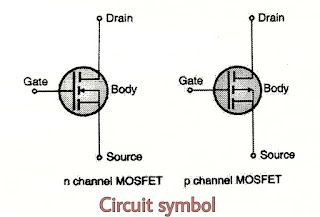
- Figure (A) shows the simplified structure of power MOSFET and Figure (B) shows the circuit symbols.

Figure (A) 
Figure (B) - The n+ p n- n+ structure shown in the Figure (A) is ow termed as enhancement mode n channel MOSFET. A structure of a p-channel MOSFET has exactly the opposite doping profile.
- The doping in the two n+ regions of Figure(A) that means the "source" and "drain" is approximately the same in both the layers and it is quite large.
- Three terminals are brought out for the user's access, which are drain, source and gate. The body terminal is not brought out, instead it is shorted with the source terminal internally.

Figure (C) - The direction of arrow on the body lead indicates the direction of current flow if the body source p-n junction were forward biased by removing the short link between body and source.
- Therefore n channel MOSFET has a P type body region and the arrow points into the MOSFET symbol. (Refer to Figure (B).
- A more simplified structure of the enhancement power MOSFET is as shown in Figure (C)
- As seen from Figure (C) the gate terminal is not connected directly to the semiconductor (P layer), instead there exists an oxide layer (SiO2) between the metal and semiconductor.
- The oxide layer acts as a layer of dielectric between the metal and the semiconductor to form a MOS (metal oxide semiconductor) capacitance at the input of the MOSFET. This MOS capacitance does not exist in the low power JFET.
- The input capacitance of MOSFET is large (greater than 1000 pF). The SiO2 oxide layer isolates the gate terminal from the body layer and gives the device insulating properties.