MOSFET Working Principle of Operation
- With gate to source voltage VGS = 0 the MOSFET is equivalent to two back to back diodes connected as shown in Figure (a). The diodes are formed between n+ and P layers as shown.
- The basic structure of MOSFET is very much similar to the BJT. The only difference is the presence of the SiO2 oxide layer that isolates the gate from the body region.
- When a positive gate to source voltage is applied, the MOSFET turns on. The operation takes place as explained as follows :


 |
| Figure (c) |
Operation of MOSFET
- The basic structure of the n type MOSFET is as shown in Figure (b).
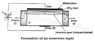
- Power MOSFET is a minority carrier device. The conduction takes place only due to electrons. Hence it is felt that the conduction cannot take place through a MOSFET from drain (n+) to source (n+) due to the presence of p layer (base layer) in between. But practically it is possible due to a phenomenon called "Inversion layer creation" which is explained with reference to Figure (c) and Figure (d).

- The operation of power MOSFETs can be divided into two steps :
- Formation of depletion region.
- Creation of inversion layer.
- The MOSFET is forward biased by connecting a positive voltage to its drain terminal with respect to source terminal and the gate is made positive with respect to the body layer as shown in Figure (c).
- The "P" layer of Figure (c) consists of a large number of holes and few electrons. The holes are majority carriers. Hence they outnumber the electrons which are minority carriers, still the number of electrons present in the "P" layer is sufficiently large.
- Due to the positive voltage applied between gate body as shown in Figure (c) these electrons are attracted towards the gate and gather below the SiO2 layer and produce depletion layer by combining with the holes that are present there.
- If the positive gate voltage is increased further, the number of electrons below the SiO2 layer will be greater than the number of holes.
- Thus the conductivity of the part of P layer close to SiO2 layer will change from positive to negative.
- That means an n type of sub layer is formed below the SiO2 layer as shown in Figure (d).
- This process is known as creation of the inversion layer, and the process of generation of an inversion layer due to the externally applied gate voltage is known as the "field effect".
- The inversion layer is also called as the induced channel. This induced channel will connect the two n+ layers on either sides of the p-region.
- In this way now the n type channel gets created in the P type body layer and conduction can take place through this layer as shown in Figure (d).
- The resistance of the induced channel is dependent on the magnitude of gate to base (body) voltage. Higher the gate voltage less is the resistance. The MOSFET acts as a variable resistor.
- With increase in the gate to body voltage, the resistance will decrease. However this resistance cannot decrease below a certain minimum value even with increase in the gate to body voltage.
- If the maximum specified value of gate voltage is exceeded then the SiO2 layer will breakdown.