Basic Structure of IGBT
Q. Draw symbol of IGBT and state one application.
Q. Draw symbols and V-I characteristics of following device : IGBT
Q. Draw the symbols of : 1. SCR 2. IGBT
Q. Draw symbol and characteristics of IGBT and its important information and application.
Q. Draw construction of IGBT. Give any two advantages of IGBT.
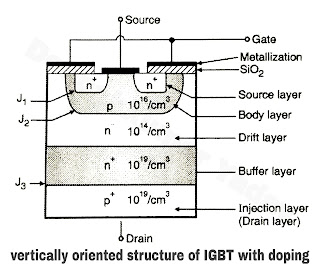
- The vertically oriented structure of IGBT is as shown in Figure (a).
- Like all other devices IGBT also uses the vertically oriented structure in order to maximize the area available for the current flow.
- This will reduce the resistance offered to the current flow and hence the on state power loss taking place in the device.
- The IGBT also uses highly inter digitated gate-source structure in order to reduce the possibility of source/emitter current crowding.

Figure (a) 
Figure (b) 
Figure (c)
- The doping levels used in different layers of IGBT are similar to those used in the comparable layers of the power MOSFET structures except for the body region. The main difference in the structure of IGBT as compared to that of a MOSFET is the existence of p+ (injection layer or drain layer) layer that form's the drain of the IGBT.
- This device also uses the n- type drain drift layer which improves its breakdown voltage capacity. This is same as that in case of power MOSFETs.
- It is also possible to make a p channel IGBT by changing the doping type in each of the layers of the device.
- The n+ buffer layer is not a must (it is an optional layer) for the operation of the IGBT and some IGBTS do not have it. (IGBTs without a buffer layer are known as symmetric IGBTS whereas those with the buffer layer are called as asymmetric IGBTs).
- The n+ buffer layer improves the operation of IGBT in two important aspects :
- It reduces the on state voltage drop across the device and
- It shortens the turn-off time.
- But the drawback is that the buffer layer reduces the reverse blocking capacity of the IGBT to a great extent.
Circuit symbol for IGBT
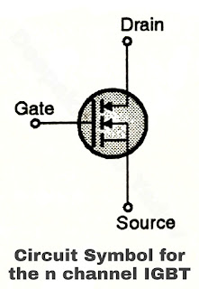
- The circuit symbols for an n channel IGBT are as shown in Figure (b) and (c). As seen from the Figure (b) and (c). IGBT is a three terminal device, gate being the control terminals.
- The directions' of the arrowheads will reverse in a p channel IGBT.
- The symbol shown in Figure (b) is almost identical to that used for the n channel power MOSFET, but with the addition of an arrowhead in the drain terminal pointing into the device.
- The symbol shown in Figure (c) is used if IGBT is considered to be basically a BJT with MOSFET gate input.
- This device has a collector and emitter instead of a drain and source. The controlling terminal however is gate (G).
- This symbol indicates that the IGBT has output characteristics similar to power BJT and input characteristics similar to the power MOSFET.